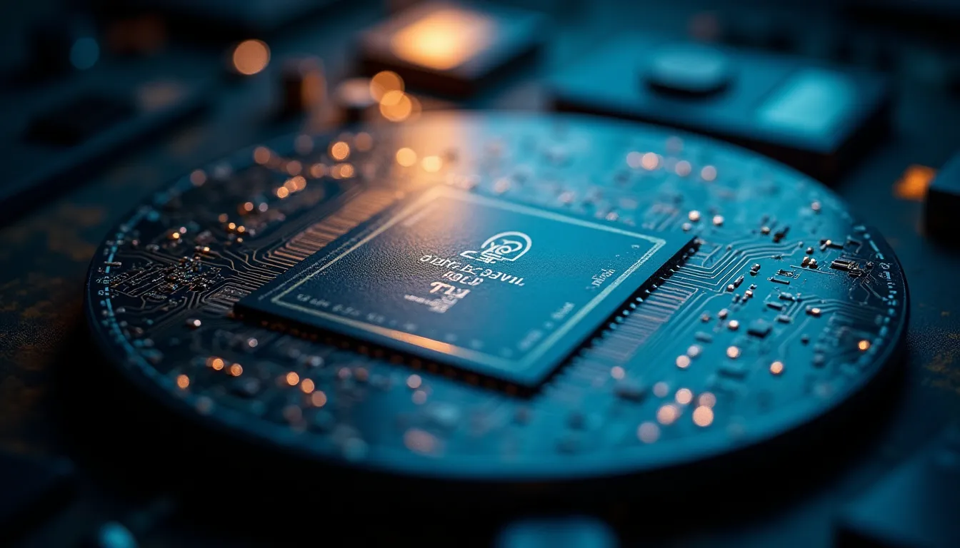
Anderon, an IBM subsidiary, has finalized a $1 billion CHIPS Act award to expand its 300mm quantum wafer foundry at Albany NanoTech Complex in New York, backed by an additional $1 billion IBM co-investment. The foundry will manufacture specialized wafers for superconducting quantum processors and other quantum modalities, marking a significant shift toward industrial-scale quantum hardware product
Key Takeaways
- Anderon finalized a $1 billion CHIPS Act award plus $1 billion IBM co-investment to expand its 300mm quantum wafer foundry at Albany NanoTech Complex in New York
- Operating as an open pure-play foundry, Anderon will manufacture specialized wafers for superconducting quantum processors, silicon photonics, and spin-qubit architectures serving external customers
- The 300mm wafer format aligns quantum hardware production with industrial semiconductor manufacturing standards and processes refined over decades, shifting quantum computing from research to industrial manufacturing
- Quantum devices require extreme purity and sophisticated tuning techniques like laser-annealed Josephson junction critical current control, making yield and coherence preservation the critical challenge
- Success will be measured by customer adoption; if yields improve and costs decline with production volume, Anderon could become the foundational supplier for the quantum computing industry
Anderon LLC, an IBM subsidiary, has finalized a $1 billion direct funding agreement with the U.S. Department of Commerce under the CHIPS and Science Act, supported by an additional $1 billion co-investment from IBM. The capital will expand operations at Anderon's 300-millimeter pure-play quantum wafer fabrication facility located at the Albany NanoTech Complex in Albany, New York. This represents one of the most significant quantum-focused semiconductor manufacturing investments to emerge from US federal CHIPS Act funding.
Anderon's Quantum Manufacturing Infrastructure
Operating as an open commercial pure-play foundry for the global quantum hardware ecosystem, Anderon manufactures specialized 300mm wafers supporting high-performance superconducting qubit arrays, high-density quantum input/output (I/O) signaling, laser-annealed Josephson junction critical current tuning, and cryogenic readout signal chain components. The designation as a "pure-play" foundry means Anderon will serve external quantum hardware customers rather than producing chips exclusively for IBM's own quantum systems—a strategic choice that positions the facility as a supplier to the broader quantum computing industry.
Initial quantum wafer production lots are currently processing through the 300mm manufacturing line. The adoption of the 300mm wafer format—the same standard used by leading-edge logic and memory fabs worldwide—represents a significant departure from quantum hardware's traditional manufacturing approach. Historically, quantum devices have been fabricated in specialized research environments optimized for experimental production. Using 300mm wafers brings quantum chip production into the same process discipline, tooling ecosystem, and yield-optimization frameworks that conventional fabs have refined over decades.
Technical Challenges and Manufacturing Standards
Applying 300mm wafer technology to quantum devices presents substantial materials and process node challenges. Quantum devices require extreme purity, novel substrate handling, and fabrication environments that differ substantially from conventional complementary metal-oxide-semiconductor (CMOS) lines. The superconducting qubits that form the foundation of many quantum processors demand coherence times—the duration a quantum state persists before decoherence—that are orders of magnitude more sensitive to defects than conventional semiconductor logic.
Josephson junctions, which form the basis of superconducting qubits, require precisely controlled fabrication parameters. Anderon's process includes laser-annealed Josephson junction critical current tuning, a precision manufacturing technique that adjusts the electrical properties of individual quantum elements post-fabrication to compensate for process variation. This capability is essential for scaling quantum processor production from laboratory prototypes to commercial manufacturing volumes.
Roadmap for Quantum Hardware Diversity
The foundry's operational roadmap encompasses expanding its 300mm fabrication capabilities beyond superconducting QPUs into complementary quantum modalities, including silicon photonics and spin-qubit architectures. This expansion strategy acknowledges that quantum computing remains a heterogeneous field: no single quantum modality has yet achieved clear dominance. Silicon photonics uses photons in waveguides to encode quantum information, while spin qubits leverage the spin states of individual electrons trapped in silicon or germanium structures. By building fabrication infrastructure flexible enough to support multiple modalities on the same 300mm production line, Anderon positions itself to serve a diverse customer base regardless of which quantum approaches prove most viable at scale.
Strategic Alignment with US Semiconductor Policy
The definitive award executes the preliminary Letter of Intent signed between the U.S. Department of Commerce and IBM in May 2026. The CHIPS and Science Act, signed in 2022, allocated $52 billion to boost US domestic semiconductor manufacturing and research. Anderon's award reflects a policy decision to treat quantum hardware manufacturing as a domestic capacity-building priority, not merely as an R&D initiative.
By establishing domestic 300mm pure-play fabrication infrastructure, the facility aims to address QPU scaling bottlenecks, strengthen onshore microelectronics supply chains, and enable production-scale wafer yield for fault-tolerant quantum computing systems. This framing shifts quantum hardware from physics research to an industrial manufacturing problem. Scaling quantum processors has long been constrained by the lack of high-volume fabrication infrastructure. By partnering with IBM and allocating substantial CHIPS Act funding, the Commerce Department is explicitly betting that quantum computing's future depends not on fundamental discoveries but on manufacturing maturity.
Context: Quantum Manufacturing and Industrial Process Node Logic
The push to manufacture quantum devices on 300mm silicon wafers represents a direct extension of the process node logic that has governed conventional chip scaling for sixty years. That logic traces back to the integrated circuit itself. The integrated circuit, independently co-invented by Jack Kilby at Texas Instruments and Robert Noyce at Fairchild Semiconductor in 1958-1959, solved what engineers called the "tyranny of numbers"—the practical impossibility of manually wiring thousands of discrete components. By placing multiple components on a single chip, the integrated circuit established the principle of density and integration that now underpins both classical and quantum chip design.
The semiconductor fabrication pipeline that produces modern chips involves photolithography, chemical processes, thermal treatments, and precision metrology refined over decades of manufacturing evolution. Anderon's foundry bet depends on that industrial apparatus being adapted and extended to quantum devices, not replaced. Quantum hardware engineers must work within the constraints and capabilities of industrial fabs rather than designing ideal processes in isolation.
Yield and Viability Questions
The critical near-term challenge for Anderon's foundry is yield—the percentage of completed wafers that meet performance specifications. Quantum devices on 300mm wafers face defect sensitivity that is orders of magnitude more demanding than conventional logic chips. A single atomic-scale defect in a cryogenic signal path can destroy qubit coherence. Scaling production without collapsing qubit coherence times is an unsolved engineering problem that will determine whether 300mm quantum wafer supply becomes commercially viable or remains a capacity-building bet on future demand.
The success of Anderon's foundry will be measured by which quantum hardware companies sign on as commercial customers. Customer adoption will indicate whether the market believes 300mm quantum wafer supply is economically viable now or represents a decade-scale infrastructure investment. This question directly bears on the long-term trajectory of quantum computing commercialization: if external quantum hardware vendors cannot achieve acceptable yield and cost economics on Anderon's 300mm line, quantum manufacturing will remain fragmented across specialized research facilities. Conversely, if yields improve and costs decline with production volume, Anderon's Albany facility could become the supply foundation for the quantum computing industry.
The convergence of large-scale federal funding, established semiconductor industrial capacity, and external foundry customers represents a structural inflection point in quantum computing: the transition from research project to manufacturing industry. Anderon's $1 billion CHIPS Act award embodies that transition and signals US policy commitment to ensuring quantum hardware manufacturing occurs domestically.
Sources
- Quantum Computing Report: Anderon Finalizes $1 Billion CHIPS Act Award to Scale 300mm Pure-Play Quantum Wafer Foundry
- The Quantum Insider: Quobly Demonstrates Key Quantum Operations on 300 mm Silicon Chip
- TechCrunch: SK Hynix reportedly in talks with Intel to build memory chips in US
- MarkTechPost: Jina AI Releases jina-ocr-v1: A 3.4B MoE Document Parser With Built-In Speculative Decoding for Low-Budget GPUs
- IEEE Spectrum: Turning Tech Talent Into Leadership Legacy
- MachineHours Encyclopedia: The Integrated Circuit — Putting Multiple Transistors on One Chip
- MachineHours Encyclopedia: How Chips Are Made — Inside the World's Most Complex Manufacturing
Frequently Asked Questions
What is Anderon's $1 billion CHIPS Act award for?
Anderon secured the $1 billion federal award to scale its 300mm pure-play quantum wafer foundry, positioning it as a dedicated supplier of quantum chip substrates for external hardware customers.
Why does manufacturing quantum chips on 300mm wafers matter?
300mm is the standard wafer size used in high-volume conventional chip fabs. Producing quantum devices at this scale allows manufacturers to use existing tooling, process discipline, and yield-optimization methods rather than building entirely new fabrication infrastructure.
What is SK Hynix reportedly planning with Intel?
SK Hynix is reportedly in talks to manufacture memory chips at Intel's US facilities. No deal terms or timeline have been disclosed by either company.
What did Quobly demonstrate and why is it significant?
Quobly showed that key quantum operations can be performed on a 300mm silicon chip made with industrial processes, suggesting quantum hardware could eventually be produced in conventional semiconductor fabs.
How does Jina AI's jina-ocr-v1 relate to GPU supply?
By designing its 3.4B parameter model to run efficiently on low-budget GPUs via speculative decoding, Jina AI reduces the dependence on high-end accelerators for document parsing workloads, which affects demand patterns across the GPU supply chain.
Get MachineHours in your inbox
AI compute and the machine economy in your inbox.